2017年7月9日星期日

World's most precise clock set for commercial countdown

precise clock
The world's most precise clock has been fine-tuned to boost radar and GPS capabilities.
The Cryogenic Sapphire Oscillator, or Sapphire Clock, has been enhanced by researchers from the University of Adelaide in South Australia to achieve near attosecond capability.
The oscillator is 10-1000 times more stable than competing technology and allows users to take ultra-high precision measurements to improve the performance of electronic systems.Increased time precision is an integral part of radar technology and quantum computing, which have previously relied on the stability of quartz oscillators as well as atomic clocks such as the Hydrogen Maser.
Atomic clocks are the gold-standard in time keeping for long-term stability over months and years. However, electronic systems need short-term stability over a second to control today's devices.
The new Sapphire Clock has a short-term stability of better than 1x10-15, which is equivalent to only losing or gaining one second every 40 million years, 100 times better than commercial atomic clocks over a second.
The original Sapphire Clock was developed by Professor Andre Luiten in 1989 in Western Australia before the team moved to South Australia to continue developing the device at the University of Adelaide.
Lead researcher Martin O'Connor said the development group was in the process of modifying the device to meet the needs of various industries including defence, quantum computing and radio astronomy.
The 100cm x 40cm x 40cm clock uses the natural resonance frequency of a synthetic sapphire crystal to maintain a steady oscillator signal.
Associate Professor O'Connor said the machine could be reduced to 60 per cent of its size without losing much of its capability.
"Our technology is so far ahead of the game, it is now the time to transfer it into a commercial product," he said.
 "We can now tailor the oscillator to the application of our customers by reducing its size, weight and power consumption but it is still beyond current electronic systems."
The Sapphire Clock, also known as a microwave oscillator, has a 5 cm cylinder-shaped crystal that is cooled to -269C.
Microwave radiation is constantly propagating around the crystal with a natural resonance. The concept was first discovered by Lord Rayleigh in 1878 when he could hear someone whispering far away on the other side of the church dome at St Paul's Cathedral.
The clock then uses small probes to pick up the faint resonance and amplifies it back to produce a pure frequency with near attosecond performance.
"An atomic clock uses an electronic transition between two energy levels of an atom as a frequency standard," Associate Professor O'Connor said.
"The atomic clock is what is commonly used in GPS satellites and in other quantum computing and astronomy applications but our clock is set to disrupt these current applications."
The lab-based version already has an existing customer in the Defence Science and Technology Group (DST Group) in Adelaide, but Associate Professor O'Connor said the research group was also looking for more clients and was in discussion with a number of different industry groups.
The research group is taking part in the Commonwealth Scientific and Industrial Research Organisation's (CSIRO's) On Prime pre-accelerator program, which helps teams identify customer segments and build business plans.

2017年7月5日星期三

Customisable Ethernet switch designed for embedded applications

The introduction of the LDD-ES8, a customisable gigabit Ethernet switch module for industrial, commercial and building automation data services, has been announced by LDD Technology. The standard LDD-ES8 module is an 8 port unmanaged Ethernet Switch on a PC/104-Plus form factor intended for use in embedded applications. It features a high performance, low latency, switch able to handle full-rate gigabit packets on all ports simultaneously.

Auto-negotiation allows each port to operate at 10/100/1000 Mbits with dual LEDs per port to indicate negotiated speed and link activity. Power is provided from the PC/104 stack or through a Molex Microclasp connector. The LDD-ES8 module is designed for fully independent operation but a USB port is provided to allow monitoring of port performance if required. Power consumption is typically 5W with all ports operating at 1 Gbit/sec.The LDD-ES8 Gigabit Ethernet switch was developed in response to a number of enquiries for custom designed products from customers who had been unable to find suitable off-the-shelf products which met their performance, footprint and end product life requirements.LDD Technology is able to offer an efficient and cost-effective customisation service in the event that customers require a design with a different number of ports or in a different form factor. The module has been designed using programmable FPGA technology which offers end users a further range of customisation options not normally found on competitive products based on dedicated devices with limited programmability.This allows customers the option of including the functionality of the standard Ethernet Switch into other designs which may require Ethernet switching as part of a more complex system with additional interfaces or processing being included in the FPGA as required.“Our LDD-ES8 Gigabit Ethernet Switch is an excellent example of how our extensive custom design experience for many different clients can be used to create a flexible standard solution for many applications” commented Malcolm Locke, Managing Director of LDD Technology.

2017年6月22日星期四

TI introduces the industry's smallest gate driver and power MOSFET solution for motor control

Texas Instruments (TI) (NASDAQ:TXN) today introduced two new device families that help reduce size and weight in motor drive applications. When used together, DRV832x brushless DC (BLDC) gate drivers and CSD88584/99 NexFET™ Power Blocks require as little as 511 mm2, half the board space of competing solutions.

The DRV832x BLDC gate drivers feature a smart gate-drive architecture that eliminates up to 24 components traditionally used to set the gate drive current while enabling designers to easily adjust field-effect transistor (FET) switching to optimize power loss and electromagnetic compliance. The CSD88584Q5DC and CSD88599Q5DC power blocks leverage two FETs in a unique stacked-die configuration, which doubles power density and minimizes the FET resistance and parasitic inductances typically found in side-by-side FET configurations.An 18-volt compact BLDC motor reference design demonstrates how the DRV8323 gate driver and CSD88584Q5DC power block can drive 11 W/cm3 power and enable engineers to jump-start their designs for smaller, lighter-weight power tools, integrated motor modules, drones and more.

Benefits of using a CSD88584/99 and DRV832x device together
Maximum power density: The combined solution delivers 700 W of motor power without a heat sink, providing 50 percent higher current than conventional solutions without increasing the footprint.
High peak current: As demonstrated by the 18-volt BLDC reference design, the smart gate driver and power block are capable of driving a peak current of up to 160 A for more than 1 second.
Optimal system protection: The combination enables shorter trace lengths and actively prevents unintended FET turn-on, while also providing undervoltage, overcurrent and thermal protection.
Superior thermal performance: The CSD88584Q5DC and CSD88599Q5DC power blocks come in TI's DualCool™ thermally enhanced package, which enables designers to apply a heat sink to the top of the device to decrease thermal impedance and increase the amount of power dissipated to maintain safe operating temperatures for the board and end application.
Clean switching: The power blocks' switch-node clip helps eliminate parasitic inductance between high- and low-side FETs. Additionally, the DRV832x gate driver's passive component integration minimizes board traces.

Tools and support to jump-start design
In addition to the 18-volt BLDC motor reference design, engineers can search for other motor reference designs that use the power blocks and gate drivers to help solve their system design challenges. The three-phase smart gate-driver evaluation module (EVM) allows designers to drive a 15-A, three-phase BLDC motor using the DRV8323R gate driver, CSD88599Q5DC power block and MSP430F5529microcontroller LaunchPad™ development kit. The EVM is available from the TI store for US$99.00.

Package, availability and pricing
The new DRV832x BLDC smart gate drivers offer peripheral and interface options for engineers to select the best device for their design: with or without an integrated buck regulator or three integrated current-shunt amplifiers. Each device option is available in a hardware or serial interface and comes in quad flat no-lead (QFN) packaging. The CSD88584/99 power blocks come in DualCool small outline no-lead (SON) packaging, with 40- or 60-V breakdown voltage (BVDSS) choices.

A layer of diamond can prevent high-power electronic devices from overheating

alayerofdiam
Powerful electronic components can get very hot. When many components are combined into a single semiconductor chip, heating can become a real problem. An overheating electronic component wastes energy and is at risk of behaving unpredictably or failing altogether. Consequently, thermal management is a vital design consideration.This becomes particularly important in devices made from gallium nitride. "Gallium nitride is capable of handling high voltages, and can enable higher power capability and very large bandwidth," says Yong Han from the A*STAR Institute of Microelectronics. "But in a gallium nitride transistor chip, the heat concentrates on tiny areas, forming several hotspots." This exacerbates the heating problem.
Han and co-workers demonstrate both experimentally and numerically that a layer of diamond can spread heat and improve the thermal performance of gallium nitride devices.The researchers created a thermal test chip that contained eight tiny hotspots, each 0.45 by 0.3 millimeters in size, to generate the heat created in actual devices. They bonded this chip to a layer of high quality diamond fabricated using a technique called chemical vapor deposition. The diamond heat spreader and test chip were connected using a thermal compression bonding process. This was then connected to a microcooler, a device consisting of a series of micrometer-wide channels and a micro-jet impingement array. Water impinges on the heat source wall, and then passes through the micro-channels to remove the heat and keep the structure cool.Han and the team tried their device by generating 10–120 Watts of heating power in test chips of 100 and 200-micrometer thickness. To dissipate the heating power, the diamond heat spreading layer and microcooler helped maintain the structure at a temperature below 160 degrees Celsius. In fact, the maximum chip temperature was 27.3 per cent lower than another device using copper as the heat spreading layer, and over 40 per cent lower than in a device with no spreading layer.The experimental results were further confirmed by thermal simulations. The simulations also indicated that the performance could be improved further by increasing the thickness of the diamond layer, and that good bonding quality between the gallium nitride chip and the diamond heat spreader was crucial to obtain the best performance."We next hope to develop a novel micro-fluid cooler of higher and more uniform cooling capability, and to achieve thermal management using a diamond layer of high thermal conductivity near an electronic gate," says Han.

2017年6月20日星期二

Wireless microcontroller integrates MCU and Bluetooth smart radio

The CC2640R2F SimpleLink ultra-low-power wireless microcontroller from Texas Instruments (TI) is in stock at Mouser Electronics. Part of TI’s CC26xx SimpleLink family of 2.4GHz devices, the CC2640R2F microcontroller features a small, single-chip system that integrates a flash-based microcontroller and Bluetooth Smart radio to target Bluetooth 4.2 and Bluetooth 5 low-energy applications.

The microcontroller combines a 61μA/MHz ARM Cortex-M3 microcontroller and a rich peripheral set that includes an 8.2μA/MHz sensor controller. The 48MHz ARM microcontroller offers 128 kBytes of flash and 28 kBytes of SRAM and supports over-the-air (OTA) updates.
The sensor controller is ideal for interfacing external sensors and for collecting analog and digital data autonomously while the rest of the system is in sleep mode.
The device includes a 12-bit analogue-to-digital converter, up to 31 general-purpose inputs and outputs (GPIOs), and built-in robust security on chip with one of the simplest radio frequency (RF) and antenna designs available.
Minimal RF expertise is required to implement the device, which helps make development and layout extremely easy.
The wireless microcontroller is available in 2.7×2.7 mm WCSP and 4×4, 5×5 and 7×7 mm QFN packages, and is designed for a board array of wireless Internet of Things (IoT) applications, including health and fitness, industrial, and home and building automation.
With ready-to-use protocol stacks (including the SIMPLELINK-CC2640R2-SDK software development kit for Bluetooth 5), the SimpleLink portfolio of wireless connectivity solutions not only offers designers maximum flexibility and support but also delivers multi-standard capabilities with code- and pin-compatibility across Bluetooth Smart, 6LoWPAN, ZigBee and ZigBee RF4CE.

2017年4月28日星期五

Microchip 8bit MCUs get up to 128kbyte flash

Microchip’s PIC18F ‘K42’ microcontrollers are available with up to 128kbyte (from 16kbyte) of flash memory in packages from 28-48 pins. Max clock speed is 64Mbit/s and there is up to 1kbyte data EEPROM and 8kbyte of SRAM.
The firm has gone big on its ‘core independent peripherals’ (CIP) to allow functions to be implemented in hardware, saving code, validation time, core overhead, and power consumption, said Microchip.
Microchip PIC18(L)F24-25K42
Intended for automotive, industrial control, IoT, medical and white goods, they include peripherals for safety critical applications including cyclic redundancy check with memory scan, a windowed watchdog timer, a 24bit signal measurement timer and a hardware limit timer, as well as up to eight hardware PWMs, complementary waveform generation for power bridges, and multiple communications interfaces.
Analogue peripherals including a zero crossing detector, constant current I/O (see below), a comparator, and a 12bit ADC with computation – the latter for automating capacitive voltage division (for touch sensing), averaging, filtering, over-sampling, and threshold comparison.
Constant current I/O
The constant current I/O feature allows the sink and source current of a pin to be set to 1, 2, 5 or 10mA. This has to be used with caution because the pin circuitry cannot dissipate much static power, so an “external resistor must be inserted in series with the load to dissipate most of the power,” said Microchip.
It has an example, with a 5V rail and a load which needs 1mA and whose voltage drop can be between 1.0 and 1.5V. The external resistor and pin circuitry has to make up 3.5-4V difference, so the resistor  needs to be chosen to drop 3.5V at of 1 mA, said Microchip, then the pin can make up the 0-500mV variable difference.
A ‘memory access partition’ supports data protection and bootloading, and the ‘device information area’ is a dedicated memory space for factory programmed device ID and peripheral calibration values.
Building blocks
  • ADC with computation
  • zero crossing detector
  • 10bit PMW
  • complementary waveform generator
  • numerically controlled oscillator
  • data signal modulator
  • hardware limit timer
  • 24bit signal measurement timer
  • configurable logic cell
  • crc/scan module
  • windowed watchdog timer
  • peripheral pin select
  • direct memory access
  • temperature indicator
  • data signal modulator
  • 5bit DAC
  • UART, SPI, and I2C

2017年4月20日星期四

lm386 amp Audio Amplifier

LM386 IC Audio sound Amplifier home made schematic and circuit diagram

Small Audio amp using LM 386 IC

This is simple and Small Audio power Amplifier project that you can make at home easily. We will make this project using a Small lm386 IC which is a 8 pin IC. You can make your own tiny simple amplifier using this lm386 IC. Due to its small size lm386 is perfect for various projects like radio amp, tiny Guitar amp amplifier.
It supports various range of supply voltage, 4V - 12V or 5V - 18V. The Audio amplification Gain can be adjusted. You can find the schematic and other additional components below. If you are planning on some hobbyist projects which includes sound systems, then amplification can be handled by this lm386 audio amp. There are many schematics available on internet based on lm386, so you can change the components based on your requirements in the schematic.
The gain is adjusted with a potentiometer. You will need an external power supply for this amplifier. Since the voltage supply can be in between 5V - 18V so you can use batteries.
This schematic was given to me by my professor, while working on an audio system in lab for some project long time ago. Hence I am sharing with you. Please don’t mind for my hand drawn model of this amplifier schematic.

Requirements for Amplifier

ComponentsValueQuantityNotes
Resistance22K1-
Resistance1R51-
Capacitor10uf1Between Pin 1 and 8
Capacitor100n1-
Capacitor330u2-
ICLM3861Amplifier

lm386 schematic for Audio Amplifier

lm386 Amplifier Schematic and Circuit Diagram


Schematic for lm386 small amp Audio

lm386 pin diagram

lm386 pin diagram for amplifier


lm386 on breadboard

lm386 amp audio amplifier circuit
Power amplifiers are something which converts low voltage input to high voltage output; hence this audio amplifier amplifies the low voltage audio into high output. During my college days I wanted to make a small audio power amp that you can put in your pocket and tune up sound in headphone hence I used this IC. For more specifications on lm386 you can refer the data sheet. A short Google on lm386 must let you to various data sheets for the same. Please refer the lm386 data sheet before changing components.
The voltage gain can be adjusted by adding a potentiometer across pin 1 and 8. Choose the speakers according to your requirement. I suggest keep gain to as low as zero when you done with schematic and then gradually tune up the potentiometer to avoid the speakers to damage. (if speakers you choose are not powerful enough). A pretty powerful amp with a low voltage battery.
PS: Just in case if you are doubtful then, pin 7 is unused pin in the IC.

lm 386 amplifier small project for audiolm 386 amplifier project picture circuit


lm 386 Audio Amplifier project
Thanks for reading

2017年4月18日星期二

Utility Power Supply

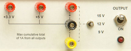
This is a standard bench power supply for prototyping electronic circuits.
Its main feature is a selection of outputs at standard fixed voltages used in electronics. Because the outputs are fixed you do not have to worry if the voltage is correct, you just plug the wire in. It is quick and easy to use.
You will probably still need a conventional variable power supply to test circuits over a range of voltages - but this is the one that you will use for day-to-day development.
It features four fixed outputs with an overall 1 amp capacity:
  • +5V and +3.3V
  • +9V or +12V or +15V
  • -9V or -12V or -15V
Design Criteria
This power supply was intended to be straight forward and easy to use without controls that needed to be adjusted. It should supply all the standard voltages commonly used in electronic circuits at 500mA or more.
Description
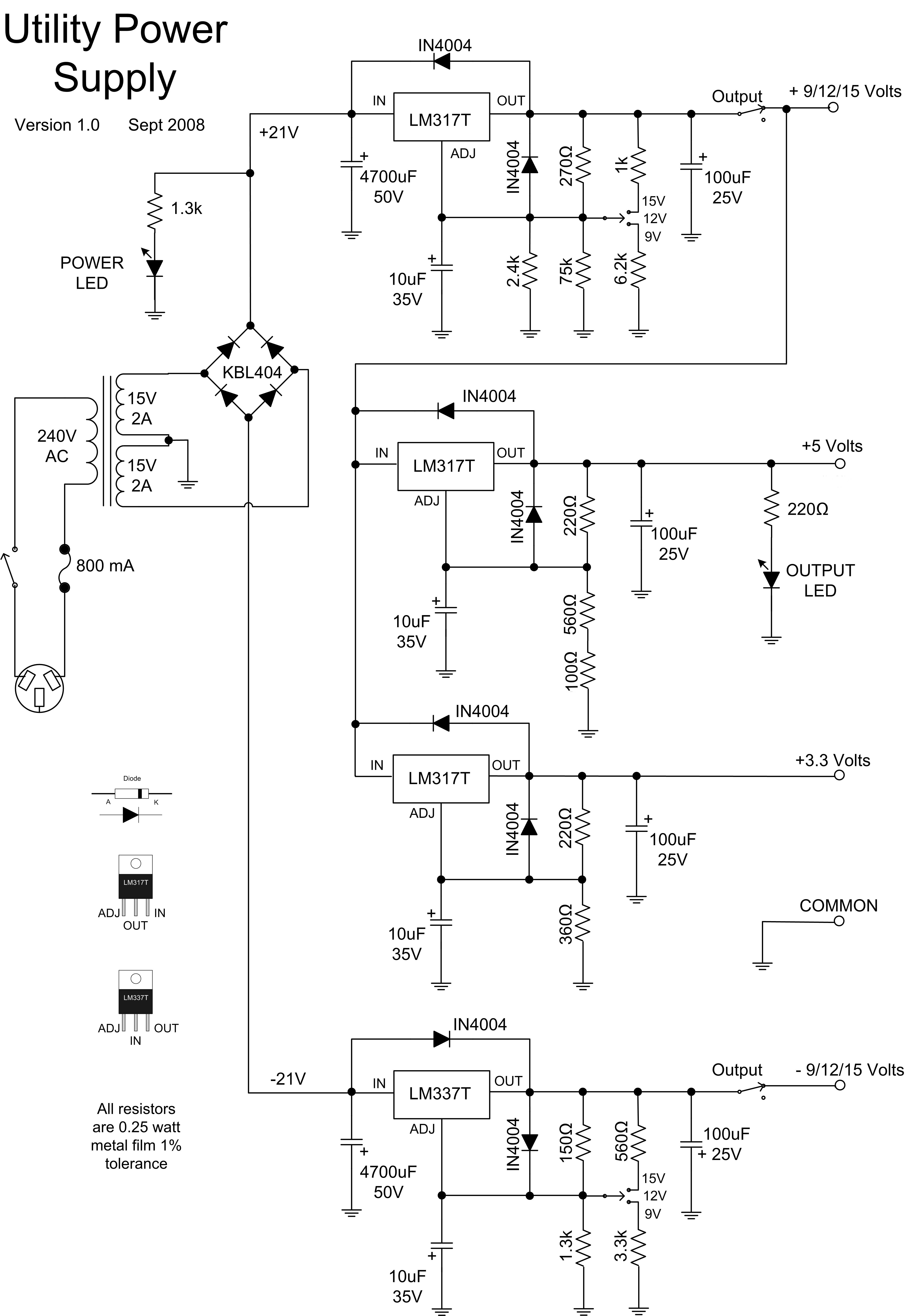
The power supply offers two fixed outputs of 3.3V and 5V, and two other voltages (plus/minus 9V, 12V or 15V) which are selected by the toggle switch.
All are referenced to the black common terminal.
The outputs are enabled by the output switch. This instantaneously disconnects the output, compared to the power switch, which, when turned off, can leave the outputs powered for some seconds due to the charge in the filter capacitors.
The Design
The circuit was designed around the LM317 and LM337 three terminal regulators. These are simple, rugged and used in many such power supplies.
The only downside is that there is no provision for current limiting... in the event of a short or something similar going wrong this power supply will attempt to drive 1.5 amps through your test circuit. Current limiting was left out because it would be difficult to properly implement and it would result in something that had to be adjusted - which was just what this project was trying to avoid.
Standard range fixed resistors are used to set the output voltages, and because of this careful attention given was to ensure that the values selected gave an result that was as close as possible to the desired voltage. In this design the maximum error due to the values of the resistors chosen is 0.89% and in most cases it is less than 0.5%. These resistors are specified as 1% tolerance and the LM317 and LM337 regulators have a tolerance of 1% also. So, the maximum error would be the sum of these (ie, 3%), but in most cases would be somewhat less. This is much better than the standard tolerance for these voltages which is 5%.
In the prototype the 3.3V output actually produced 3.299V, an error of 0.03% (close to the error of the measuring DMM). The 5V output actually produced 4.994V or an error of 0.12%.
Variable resistors could have been used to trim the output voltage to a precise value but, given the results, that would have been unnecessary and would have introduced a source of unreliability.
Schematic
This schematic is also available from the download section at the end of this page.
The circuit is reasonably conventional. The two diodes around each regulator are there to protect the regulator from unusual events such as the output being connected to a negative or higher voltage.
No specialised components are used, the voltage select switch (+/- 9/12/15V) is a center off switch with three positions. All resistors (with the exception of the current limiting resistors for the LEDs) should be 1% metal film.
The +5V and +3.3V regulators take their input from the output of the regulator which supplies the +9/12/15 volts. The reason for this is to spread the heat dissipation involved in supplying a low voltage like 3.3V across two regulators rather than one. For example, when the top regulator is set to 12V and the 3.3V regulator is supplying 1 amp both the regulators will be dissipating approx 9 watts. Whereas, if one regulator was used to supply 3.3V from the 21V supply the dissipation in that one regulator would be almost 18 watts.
Construction
The power supply was built into a small bench case with each regulator and its associated components assembled on small pieces of veroboard. The regulators were bolted onto a heatsink and the veroboard that they were attached to were simply supported by the legs of the regulators. The power supply was so simple that nothing more sophisticated than that was required.
Each regulator must be attached to a substantial heatsink. If a single heatsink is used then it should be of reasonable size as it could be called on to dissipate up to 20 watts. Typically a heatsink with less than 2.5 degrees per watt should be selected. For example, Altronics H0574 or Jaycar HH-8570. Note that insulating grommets, mica shims and heat conducting grease should be used to electrically isolate the mounting tab of each regulator from the heatsink and each other.
If separate heatsinks are used for each regulator then less than 5 degrees per watt heatsinks should be used. Also, insulating hardware is not needed if the heatsinks are electricially isolated from each other (e.g. attached to the plastic case).
The front panel was made by designing the panel in Visio and printing the output onto paper with a sticky backing that was suitable for laser printers. This printout was trimmed and stuck onto the drilled front panel. Finally a layer of clear sticky film (often used to protect book covers) was stuck over the paper and trimmed to size.

2017年4月14日星期五

Easy High Voltage Power Supply

Easy High Voltage Power Supply
This article will walk you through making a High Voltage Power supply .
Before attempting this project, be aware of some simple Safety Precautions.
1. Always Wear electrical gloves when handling the High Voltage Power supply.
2. The Voltage produced by this Power supply is not lethal, but can be damaging.So it is advisable to keep one hand in your pocket,or behind you while using it.(especially if you ignored Precaution #1).
3. Flyback transformers tend to hold charge for days after powered off, so always make sure to discharge(mentioned later on) it before touching the output wires.
Finally,i am not responsible for whatever damage(if caused) by this project to you.
PLEASE GO THROUGH THE ENTIRE INSTRUCTABLE BEFORE ATTEMPTING THE PROJECT.

Step 1: Gather the Materials

Gather the Materials
MATERIALS REQUIRED:
1. Flyback Transformer
You can get this from any CRT TV or Monitor.Be careful while removing it,as it can hold a charge for days after it is powered off.(precaution #3)
Alternatively,you can also buy it online, but it is rather expensive.(at least 20$)
2. Electronic Ballast
you can get this in a traditional tube light set.
You can also buy this online ,but make sure it is suitable for your country's power outlet.
3. Electrical plug with wire
you need this to connect your power supply to the power outlet of your house.
you can make one with a plug head and some wire,or buy it online.
4.Electrical tape(black and yellow)
you need colored tape only for the decoration part, but you need to have it for insulation.
TOOLS REQUIRED:
1.Soldering Iron
you may be able to manage without one,but it is highly recommended.
You need to be able to measure resistance to find out the primary coil of your flyback transformer.
3.Wire strippers and other common tools
you will need some common tools like screwdrivers and pliers.

Step 2: Identification

Identification
IDENTIFYING THE PINS OF YOUR FLYBACK TRANSFORMER
*If you can get a Datasheet for you flyback transformer,it will have the pin out.
MAKE SURE THAT THE DATASHEET IS FOR YOUR TRANSFORMER.
To find the datasheet, you need to know the part number. It may be written on the transformer or even in the service manuals of the device you acquired it from.
*If you couldn't find a datasheet for your transformer you have to identify the pins manually,by following the steps given below.
-The High Voltage output positive wire will be connected to a suction cup.You can keep it, but i chose cut it off.
-The HV output ground(negative) will be found later on.
-You need to find the Primary coil of the transformer. For this measure the resistance between every two consecutive pins. The pair of pins with the resistance closest to 1 ohm are the two ends of the primary coil.
Refer to a YouTube Video If you are confused. There are quite a few dedicated to this topic.
IDENTIFYING THE OUTPUT TERMINALS OF THE BALLAST
You need to open the ballast to get two of the four output wires that are not connected to a capacitor. Refer to the images.

Step 3: Connecting Them All Together

Connecting Them All Together
The two wires in the ballast that don't go to the capacitor are connected to the primary coil of the flyback. Connect the plug and wire to the input of the ballast. Polarity doesn't matter as it is AC. Make sure to insulate the connections from each other and from you.

Step 4: Finding the Negative(ground) Pin

Once all the connections are made, wear your gloves and boots,then power it up. It is normal for the ballast to create a small whirring sound.
-Use pliers to carefully move the HV+ wire near all the pins of the flyback, except the primary coil pins.
-The negative pin and the Positive wire will create electric arcs.
-Disconnect it from the wall outlet, then touch the HV+ wire to the negative pin to DISCHARGE the flyback.
-Now,it is safe to touch.
-Solder a thick wire to the negative pin for easier access to it.
-High quality wire is recommended to prevent any leaks.(High voltage of electricity can get through low quality rubber and plastic)


Step 5: Encasing and Decoration

Encasing and Decoration
Choose a good box that can accommodate both the ballast and the transformer.
-Avoid using a metal box for electrical projects
I chose a cardboard box that could fit both the ballast and the flyback. Then, i used black and yellow electrical tape to make the Eye-catching design. To make it, start with black tape from one corner of a side(of the box) to the other. Then use yellow tape along the edge of the black one on both of it's(black tape's) sides. Then continue using alternative colors of tape. Once you get to the edge of one side,continue to the other with the same strip for better results.
You can make holes in the box for the wires, but i jut brought them out through the corners.
I also had an extra wire in my transformer,which i guess goes to the high voltage capacitor that is built into my transformer. You should have only three wires coming out of the box, the HV+,HV- and the power input(that goes to the wall outlet).
HERE is the link to the video shown above.
You can use a high voltage power supply for various other projects like a Jacob's ladder or a Tesla coil.

2017年4月12日星期三

The Simplest Amplifier Circuit Diagram

I have been looking for a good stereo amplifier circuit diagram for a long time. I am not a HiFi geek, I just wanted to build a simple stereo amplifier that could drive some speakers for my desktop computer.
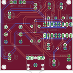
stereo-amplifier-board-layout
All the schematic diagrams that I could find seemed to involve lots of hard-to-find components or you had to use it together with a pre-amplifier or some other amplifier stage. It was always something that made me hesitate.
But recently I found this awesome little chip called TEA2025! You only need a few capacitors to make a decent stereo amplifier out of it. It is so simple to build that I put it together on a strip board in just a few hours.

2.5W * 2 Stereo Amplifier

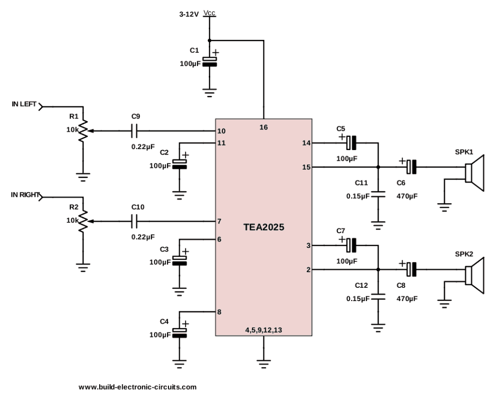
The amplifier circuit diagram shows a 2.5W * 2 stereo amplifier. You can also make a 5W mono amplifier out of it. (Check out the TEA2025 datasheet for more information on that)
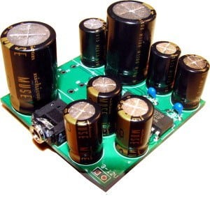
Stereo Amplifier Circuit Board
On the input side, you should use a dual potentiometer. A dual potmeter allows you to connect both left and right channel on one potentiometer.
This amplifier is great to use together with some speakers to get sound on your desktop computer. I am thinking of putting one in my kitchen and in my bathroom also. Then maybe hook them up to my home network and stream music from a server =) There are many possibilities when you can make such a cheap amplifier.

Amplifier circuit diagram and parts list

A Stereo Amplifier Circuit Diagram

Parts list

PARTVALUEDESCRIPTION
C1100µFPOLARIZED CAPACITOR
C2100µFPOLARIZED CAPACITOR
C3100µFPOLARIZED CAPACITOR
C4100µFPOLARIZED CAPACITOR
C5100µFPOLARIZED CAPACITOR
C6470µFPOLARIZED CAPACITOR
C7100µFPOLARIZED CAPACITOR
C8470µFPOLARIZED CAPACITOR
C90.22µFNON-POLARIZED CAPACITOR
C100.22µFNON-POLARIZED CAPACITOR
C110.15µFNON-POLARIZED CAPACITOR
C120.15µFNON-POLARIZED CAPACITOR
TEA2025TEA2025BAmplifier chip
SPKR14-8 Ohm speaker
SPKR24-8 Ohm speaker
R1+R210KDUAL Potentiometer
Total cost of the components (excluding speakers) is about $9. The most expensive component is the potentiometer (about $3-4).

Download Eagle schematics and board layout

Here is the schematics (Eagle), PCB board layout (Eagle) and Gerber files. This board was made to comply with the design rules of Seeed Studio (May 2013).